This is a review guide for Prof. Leo Lorenz's Power Semiconductor course. May you all have satisfying results!
Author: CHENG Li, GUO Yao
There are thousands of ways lying on the earth, but the prudence is the first rule. If one didn't observe the specification, then somebody is going to be in tears.
Two major categories of power devices
What's the 2 major categories of power devices?
Unipolar devices & Bipolar devices
A majority carrier device (e.g., a Schottky diode, a MOSFET, etc.); this uses only one type of charge carriers.
A minority carrier device (e.g., a thyristor, a bipolar transistor, an IGBT, etc.); this uses both majority and minority carriers (i.e., electrons and electron holes).
How to differentiate them ?
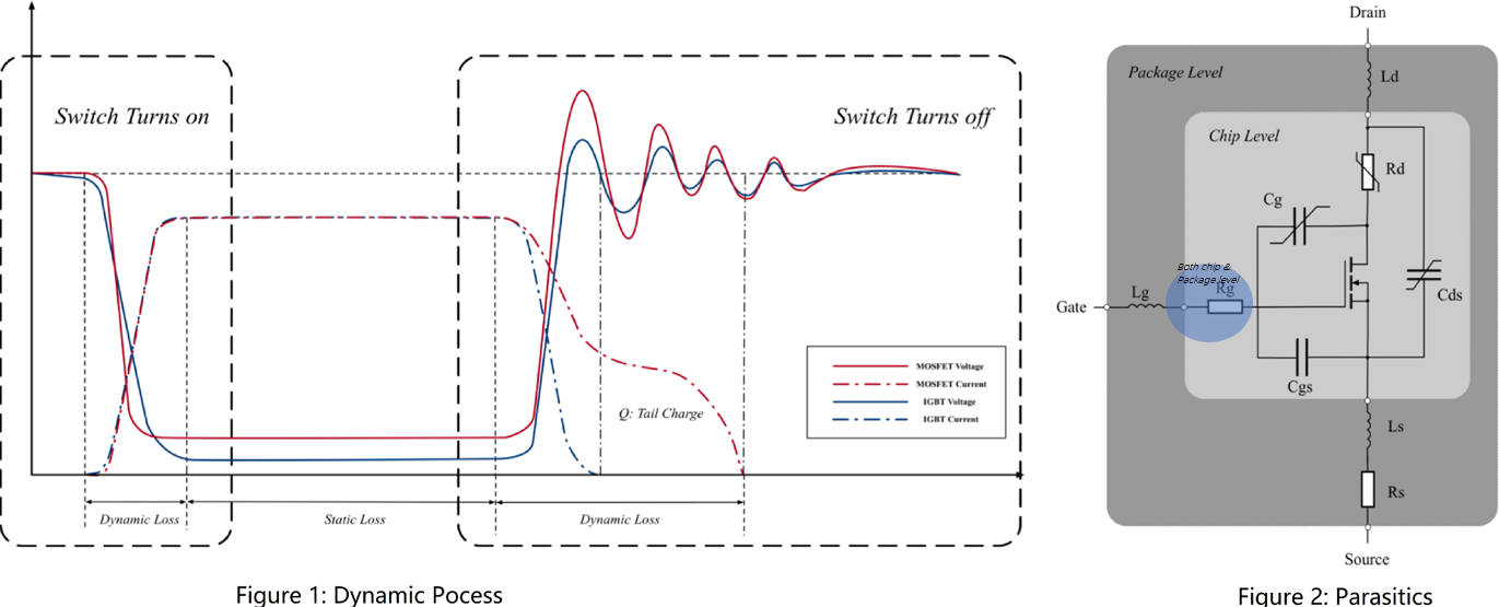
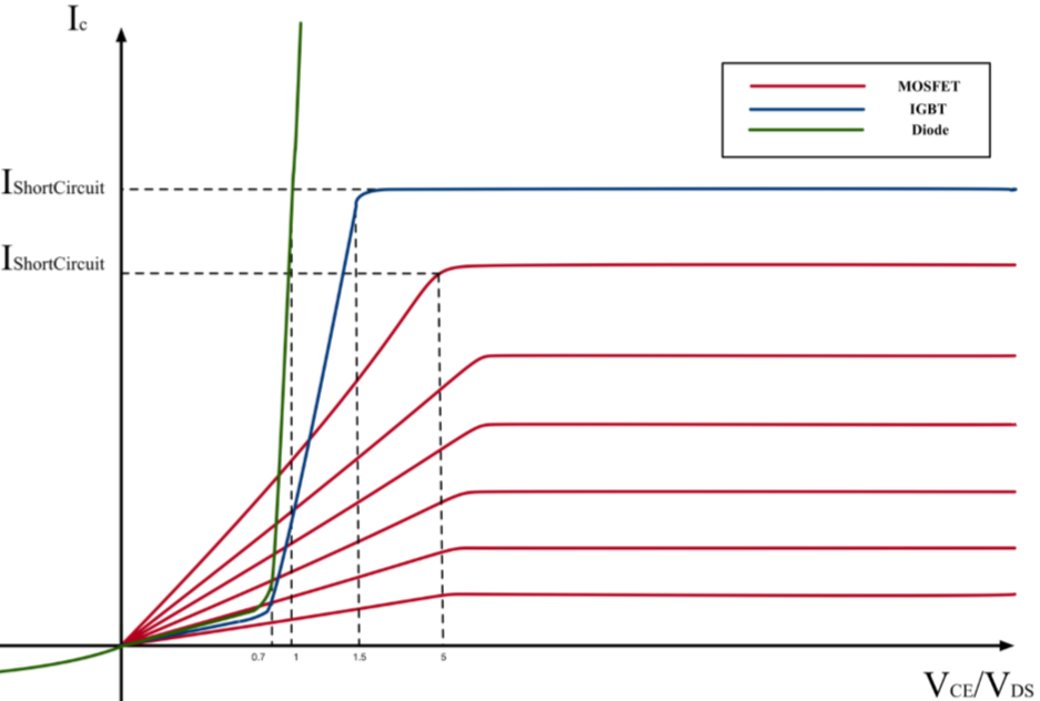
As is shown in Figure 1:
- Static differences: because of the conductivity modulation, bipolar device has smaller resistor which leads to lower on-state loss
- Dynamic differences: because of these carriers which help reduce the on-state resistor, when turned-off, bipolar device always has tail charge more of less, which leads to higher dynamic loss; when turned-on, bipolar devices have a threshold voltage, while MOSFETs can be turned on immediately.
Triggerable and controllable devices (explain difference)
Triggerable devices: diodes, GTOs, Thyristors
- Current pulse to turn on
- No way to turn off
- No limitation of current
- Lower power loss —— Voltage drop is lower than the controlled devices
Controllable devices: MOSFETs, IGBTs
- High level voltage to turn on
- Low level voltage to turn off
- Current limit function
- Higher power loss —— Voltage drop is higher
Parasitic parameters
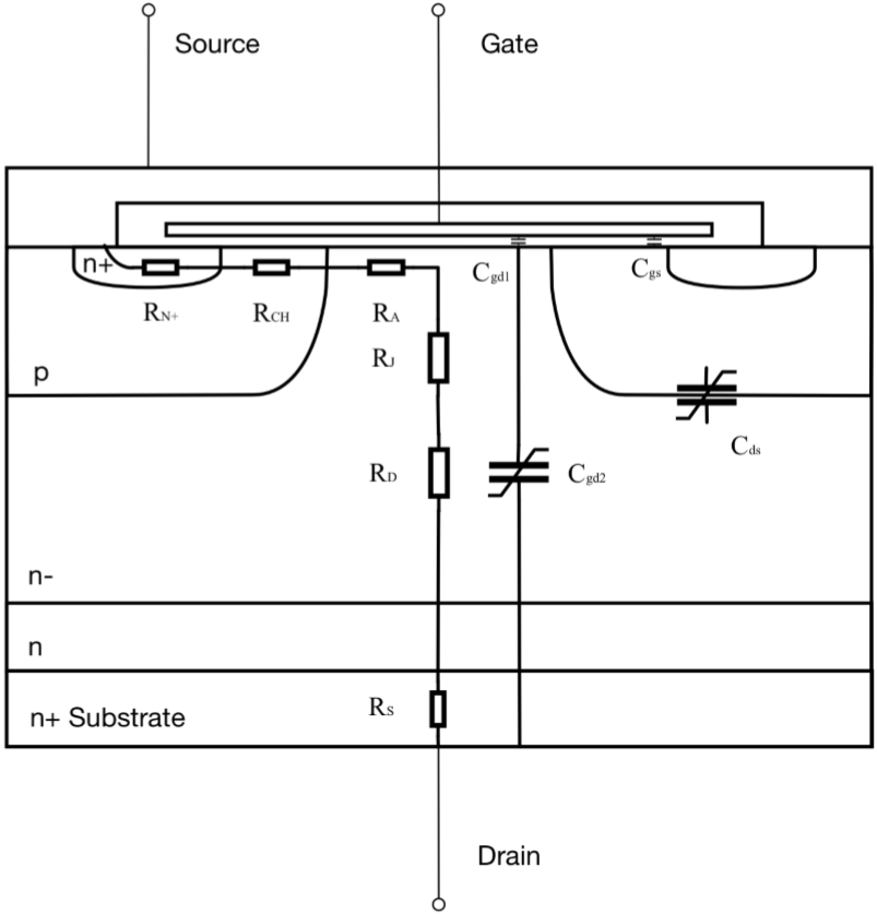
What are MOSFETs & IGBTs' key parasitic parameters on chip level?
As is shown in Figure 2, key parasitic parameters on chip level are , (or said ), , and .
Among these parasitic parameters, the parasitic capacitances have big influences on the dynamic performance of the devices.
What are MOSFETs & IGBTs' key parasitic parameters on package level?
As is shown in Figure 2, key parasitic parameters on package level are , , , , and .
Among these parasitic parameters, the parasitic inductances have big influences on the dynamic performance of the devices.
What's the impact on Source & Drain Stray Inductors?
Stray Inductor means the parasitic inductance on the wire in the package level. There is the formula:
So there exists a voltage drop over and .
For the source inductor , because of the formula, if the switch turns on, there is a current flow from gate to source, thus is charged and it takes up voltage, which may make the gate voltage lower and slow down the speed of turning on. If the switch turns off, it will cause a minus voltage of the drain, which make the turn-off process more difficult.
For the drain inductor , because of the formula and the function of free wheeling, if the switch turns off, generates a voltage overshoot, which may damage the device. We can see the voltage oscillation during the period of turning off. In order to keep the device safer, a voltage stabilizing diode is added. If the switch turns on, than it will make the drain voltage lower, which will slow down the speed of turning on.
What is the impact on Feedback Capacitor (of MOSFETs)?
The Feedback Capacitor means the Miller capacitor, also called the Reverse Transfer Capacitance () in most datasheet, which is the capacitor from drain to gate ( only). There is the formula:
consists of 2 parts, one is a constant oxide capacitor and the other is a non-linear space charge capacitor. Because of the formula above, generates a current flow, and because of the existence of which holds up the voltage, the gate voltage is hard to reset, thus it may cause the device can't turn off.
Thermal parameters
What are the parameters impacting on the junction temperature?
Take an IGBT case as an example, from the top layer to the bottom layer, there are:
The chip, the solder between chip and DCB, the DCB (Cu-Ceramic(Al2O3)-Cu structure), the solder between DCB and the base plate, the base plate.
In most conditions, a whole IGBT module includes the chip, the case and the heatsink, so the thermal grease between the base plate and the heatsink, the heatsink, these two layers are added to the structure of an IGBT module.
The thermal resistors and thermal capacitors impact the junction temperature. They are the abstract of the different layers in a module. In steady state, only the thermal resistors decide the temperature drop between different layers. The main temperature drops exist between the junction and the case (), the case and the heatsink (), the heatsink and the ambient (), so the main thermal resistors can be defined between these layers, i.e. , , and a constant temperature drop between the heatsink and the ambient can be specifically assigned.
Show thermal equivalent circuit diagram.
To reveal the temperature drop off all the layers, the equivalent circuit shows below:

While to simplify the thermal path, considering the steady state equivalent circuit, which is shown below:

What is the most critical interface?
In power cycling, 5 major internal connections are stressed with the temperature, which are:
- Cracks from bond wires
- Solder between chip and DCB
- Cracks in DCB joint
- Solder between DCB to base plate
- Thermal grease between base plate and heatsink
And from the heat distribution, the ceramic part of DCB, the thermal grease and the heatsink bear most of the heat. So we can say that the ceramic part of DCB and the thermal grease are the most critical interfaces.
In another side, the ceramic is in the package, so the only part we can deal with is the thermal grease. So we can also say that the thermal grease, or the interface between the case and the heatsink, is the most critical.
What is the impact on chip size for junction temperature?
The factors which impact the junction are the thermal resistor and the thermal capacitor, which are:
In steady state only the thermal resistor has the influence, so we hope should be as small as possible. We can increase the cross-section area, or reduce the thickness, from which the former one is easier to realize. So the large cross-section area can reduce the junction temperature, under the same power rating. The increase of area can also enlarge the capacitance, but the time constant will not be effected, so it doesn't matter.
Specify the main contribution of losses in power devices during operation.
When it comes to a power source of high voltage, such as , over voltage is taken up by the epitaxy resistor (); if a power source is in low voltage, such as , the epitaxy resistor takes up one third voltage, the charge resistor takes up one third, and the last of the one third voltage is taken up by the rest of resistors (). That is the contribution of the on-state loss.
In an entire switching process, the loss can be described by the formula below:
Among these losses, is small enough to be neglected. For MOSFET, it has lower dynamic losses but higher static loss thus it is widely used in high switching frequency domain. For IGBT, it has high dynamic losses but low static loss thus it is widely used in low switching frequency domain.
Certain technics
Why we have a Si-limit for P-MOSFET?
There exists a formula:
in which is the on state resistance, is the cross-section area, is the length of the space charge area, is the doping concentration of the donner, is the mobility of the electrons.
If the decreases, then under the same voltage, will increase, so the on state resistance will increase, and the power loss will be remarkable. On the other side, if is high, than the breakdown voltage will not be high enough, the breakdown will be easy.
This trade-off is inevitable. To loosen this trade-off, we must exceed the Si-limit.
(Another explanation is, the Super Junction Structure can reduce the Miller capacitance , and thus the speed of the switch can be improved. Thus to exceed the Si-limit.)
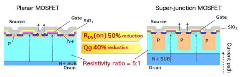
How to exceed the Si-limit (Show device structure)?
Except for changing to a bipolar device, the only way for unipolar devices to exceed the Si-limit is to use the Super Junction Structure.
How to improve the dynamic & static performance of IGBT?
Trench structure.
How to compare HV SiC MOSFET & IGBT?
Compared with the common IGBTs, the MOSFETs have larger on-state resistance and lower power rating, but it can reach higher switch speed. The use of HV SiC MOSFET can partly overcome the drawbacks of the common MOSFETs.
Compared with IGBTs, the HV SiC MOSFET has the same level of on-state resistance and power rating, while it has faster switch speed.
Double pulse testing (explain requirement)
The double pulse testing is to test the turn-on and turn-off process of the lower switch, and the reverse recovery process of the upper freewheeling diode, at the same time.
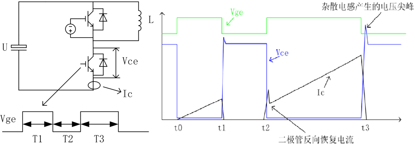
The first pulse is to build the current, then at the point of , the turn-off process of the lower switch (when the on-state current is not so high) can be seen. Because of the large inductance value of , the current flows through it will not change when the time is between and . At the time of , the freewheeling process of the upper diode, and the turn-on process of the lower switch can be seen. The second pulse is to build the big current, to test the turn-off process of the lower switch in a big current condition. The voltage peak
So at the big current condition, the is enough obvious.
How to compare Si Power MOSFET & Super Junction Device?
- Cell structure: in Section How to exceed the Si-limit (Show device structure)?
- Static performance: the Super Junction MOSFET has larger breakdown voltage, while this advantage will not worsen the on-state process. Its on-state resistance has at least the same level of value as that of the Si MOSFET.
- Dynamic performance: The of the Super Junction Device is smaller, so the dynamic performance is improved.
What is the main reason for going towards WB-devices?
Take the SJ devices and SiC transistors of the same voltage capability, for example:
- On-state
- Drift layer
Diodes, MOSFETs and IGBTs
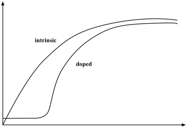
Basic characteristics of doped Silicon and intrinsic conductivity
Compared to the intrinsic conductivity, doping help silicon’s characteristic not so sensitive to temperature at low temperature case. In low temperature environment, it performs at nearly constant value.
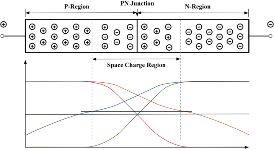
Carriers distribution of PN junction
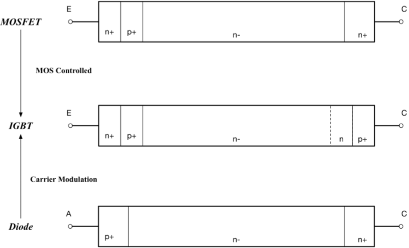
Basic structure of diodes, MOSFETs, and IGBTs
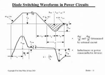
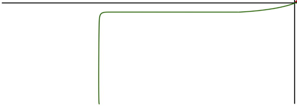
Switching behavior of diodes (turn-on, turn-off)
When turned off, there exist a large for the diode.
Compare Si-diode & SiC Schottky Diode (dynamic performance)
Compared with Si diode, the SiC Schottky Diode has faster switch speed, lower breakdown voltage, higher on-state resistor, higher leakage current, smaller reverse recovery current.
What is the main difference of MOSFET and IGBT?
- Cell structure:
- Static
- Dynamic
Why IGBT is named a carrier modulated device?
The minority carriers (holes) injected into the collector region will move to the drift region during forward conduction, then the resistance of the drift region is considerably reduced (conductivity modulation effect).
Switching behavior of MOSFETs and IGBTs (turn-on, turn-off)
When turned on, the MOSFETs and the IGBTs will have the Miller plateau in the gate signal, and the output voltage will decrease after the gate signal reaches the Miller plateau. When turned off, the IGBTs have the tail current. The transient time of the switching process of MOSFETs is smaller than that of IGBTs. The dynamic process can be seen in Figure 1.
I/V characteristic
I quadrant:
III quadrant:
The reverse breakdown voltage of the IGBT is lower than that of the diode, so the freewheeling diode is also necessary in the structure of the IGBT.
Dependency of of MOSFETs
According to equation , it is depended on the cross-section area, the length of space charge area, the doping concentration, and the temperature. A point to be paid attention to is, the has a positive temperature coefficient. That is because the mobility of the hold and the electron decrease with increasing temperature.
The other corresponding points is shown on the section Specify the main contribution of losses in power devices during operation.
Main MOSFET capacitances
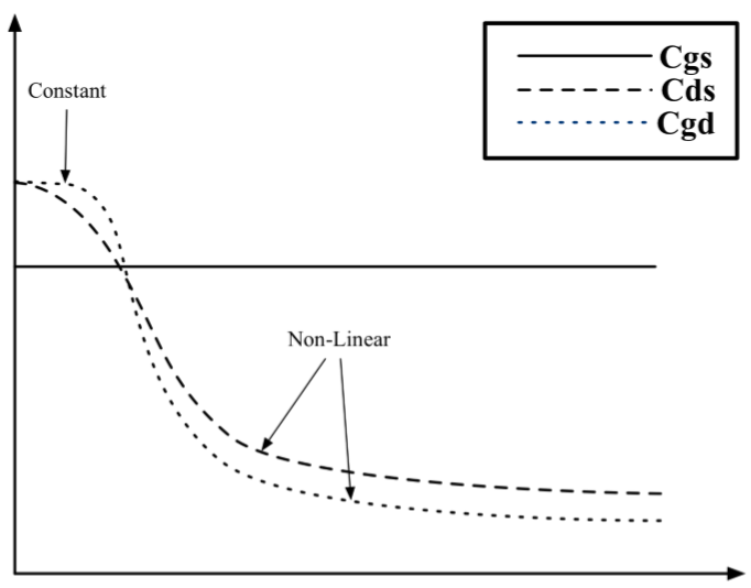
- : Oxide capacitor, constant
- : Space charge capacitor, non-linear
- : Mainly oxide capacitor, constant
- : Space charge capacitor, non-linear
How to modify the switching waveform of diodes, MOSFETs and IGBTs (soft switch, IGBT fast turn on and slow turn off)
- IGBT fast turn on and slow turn off: the time of the turn-on and turn-off is depended by the . There is a formula:
If increases, then decreases, the time of switch extended. So the fast turn on and slow turn off can be realized by the parallel of a resistor and a resistor in series with a diode.
- Soft switch